_白-120x57.png)
Toward the Dawn of Space Semiconductors
As a RIKEN-born startup, we have achieved world-class output levels in the compound semiconductor AlGaN (Aluminum Gallium Nitride) through our proprietary band engineering technology.
Building on this crystal growth expertise, we are now working to develop a platform for manufacturing ultra-high-quality crystals of diverse compound semiconductors — not limited to AlGaN — that are difficult to produce under Earth's gravity, by leveraging the microgravity environment of space.
SCIENCE OF MICROGRAVITY
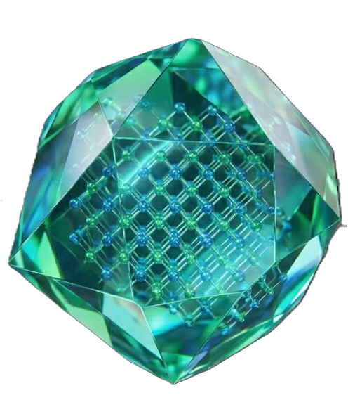
Suppressing convection, reducing the effects of sedimentation and buoyancy.
Ground-based crystal growth faces a fundamental challenge: thermally-driven convection caused by gravity introduces compositional non-uniformity and defects. In the microgravity environment of space, these effects are significantly reduced, enabling crystal growth conditions that more closely approach the ideal.
✓ Reduction of Crystal Defects
By suppressing convection-driven disturbances in the melt, we expect a reduction in crystal defects (dislocations) that govern the characteristics of compound semiconductors.
✓ High-Purity Compound Formation
Under a stable diffusion environment, the incorporation and segregation of impurities are suppressed, enabling the realization of homogeneous, high-purity crystals.
✓ Unlocking the Material's True Performance
Through improved crystal quality, performance degradation caused by defects is minimized, allowing the intrinsic capabilities of the material to be more fully realized.
CHALLENGES
A New Option for Semiconductor Manufacturing.
The quality challenges of convection and segregation caused by gravity have long been inherent to ground-based manufacturing.
The microgravity environment of space significantly suppresses these root causes.
We aim to manufacture in space semiconductors of a quality that is difficult to achieve on the ground.
Following demonstration aboard the International Space Station, we will expand toward an autonomous flying manufacturing platform.
We will deliver this semiconductor manufacturing technology — one that transcends the constraints of Earth — from Japan to the world.
TECHNOLOGY
Space Manufacturing Platform
We are advancing the development of manufacturing processes in space, working to establish our own proprietary manufacturing technology.
Semiconductor Design Technology
We possess proprietary band engineering technology for drawing out the full characteristics of compound semiconductors.
Proprietary Technology Foundation
We possess deep technical knowledge accumulated through collaboration with research institutions including RIKEN, backed by a team with expertise spanning both space and semiconductors.
SOLUTION
Power Challenges in AI & Data Centers
In AI data centers where power consumption is surging due to the massive volume of data communications, high-speed, low-power optical communication devices using compound semiconductors contribute to resolving this energy challenge.
Foundation of Next-Generation Communications
Next-generation communications advancing toward higher speeds and greater capacity face performance challenges on both the radio wave (high-frequency) and optical (optical communications) fronts. Compound semiconductors cover both domains with high efficiency, supporting the communications infrastructure of the 5G/6G era.
Dual-Use Technologies Supporting National Security
Compound semiconductors are also used in defense and national security applications, such as radar and aerospace equipment. They deliver exceptionally high performance and reliability even under harsh conditions, and as dual-use technologies that transcend the boundaries between civilian and defense sectors, they provide strong support for the security of the nation and society.
TEAM
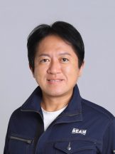
Kazuki Iimura
Representative Director & CEO
From 2022 to 2025, he served as Team Leader (PI) of the "Virus Inactivation LED System Research Team" at RIKEN, and founded the company with the goal of bringing that technology to society. After graduating from Nihon University, he experienced a TSE Mothers listing while working at a startup, and led business operations as head of the strategic investment division. He subsequently founded multiple venture companies. In 2017, his selection by the JAXA Space Exploration Innovation Hub marked the beginning of his ultraviolet LED research. Within the same hub, he also worked on the development of a "Space Virus Removal System." Armed with a proven business track record and deep expertise in deep tech, he drives the company's space manufacturing business with exceptional force.
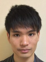
Yuri Itokazu, Dr.Eng.
Director, CRO
As a Research Associate at RIKEN, he conducted research on improving the efficiency of deep ultraviolet light-emitting devices and laser technologies. He contributed to the advancement of deep UV light source technology through his involvement in RIKEN's Far-UVC LED research, which achieved a world record in 2022. Drawing on that experience and expertise, he assumed the role of Director, CRO of the company in 2023. With band engineering technology — which enables structural control at the atomic level — as his core competency, he plays a central role in semiconductor design and technology development. He holds a graduate degree from Saitama University.
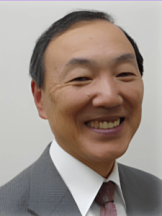
Kinoshita Kyoichi, Dr.Sc.
Director of Technology
After his tenure at Nippon Telegraph and Telephone Public Corporation (now NTT), he went on to serve as an Invited Researcher at the National Space Development Agency of Japan (now JAXA) and as a Senior Researcher at the Institute of Space and Astronautical Science, among other roles. Over many years, he has been engaged in research on crystal growth and materials development for semiconductors utilizing the space environment. He has led numerous space projects, including crystal growth experiments aboard "Fuwatto 92," small rockets, and the International Space Station (ISS). In recognition of his contributions, he has received paper awards from the Japan Association for Crystal Growth and the Japan Society of Microgravity Application, among others. He leads the company's space manufacturing technology. He holds a graduate degree from Waseda University.

Muhammad Abdul Aziz Al Mujahid, Ph.D.
専任研究員
Specializing in numerical simulation grounded in physical modeling and statistical analysis, with strong implementation skills in numerical computation and data processing using C, R, and Python. Has built a track record in optimization research integrating qualitative inquiry and quantitative analysis. Joined the company as an intern while enrolled in the Graduate School of the University of Tokyo, and transitioned to a full-time position upon graduation. At the company, he combines CFD (computational fluid dynamics) expertise with AI and data analytics to develop on-orbit simulation frameworks for crystal growth processes in microgravity environments. Driving end-to-end ownership from problem identification through implementation and validation, he supports the company's space manufacturing technology from the numerical analysis front. He holds a B.Sc. in Physics from Universitas Padjadjaran (Indonesia) and a graduate degree from the University of Tokyo.
MESSAGE
"The answer lies beyond gravity."

In 18th century Britain, the technique of dropping molten lead to produce perfectly spherical bullets was a pioneering example of manufacturing utilizing microgravity.
Today, what we are taking on is a "semiconductor process through microgravity."
Manufacturing has always been a continuous confrontation with gravity. In ground-based crystal growth, gravity-induced thermal convection, atomic segregation, and lattice defects remain significant barriers to achieving higher quality.
As the space industry shifts toward "on-orbit utilization," we harness the microgravity environment to bring new possibilities to semiconductor manufacturing through precision control in a convection-suppressed, levitated state.
This is a challenge that can only be achieved through the coming together of experts across disciplines. We refrain from excessive proclamations, believing that results are what speak. Beneath that quietness, a challenge that will transform the industries of the future moves forward steadily, every single day.
Kazuki Iimura
CEO & Founder, BEAM Technologies
COMPANY
| Company Name | BEAM Technologies, Inc. |
|---|---|
|
Location |
(Head Office) 9-3 Nibancho, Chiyoda-ku, Tokyo (Laboratory) Wako RIKEN Incubation Plaza 108, 2-3-13 Minami, Wako-shi, Saitama |
|
Representative |
Representative Director Kazuki Iimura |
|
Founded |
March 2022 |
|
Business Description |
Space-Based Semiconductor Manufacturing Platform Business |
|
Shareholders |
Management, UntroD Capital Japan, Tokyo University of Science Innovation Capital, PE&HR (Saitama Resona Startup Support Investment Limited Partnership), DG Daiwa Ventures, Gogin Capital, Hamamatsu Photonics Corporate Venture Capital, Shinnichi Kogyo, Midtown Frontier Fund, Individual Investors |